Computer chips are always getting smaller and faster – right? Historically, this has been the trend.
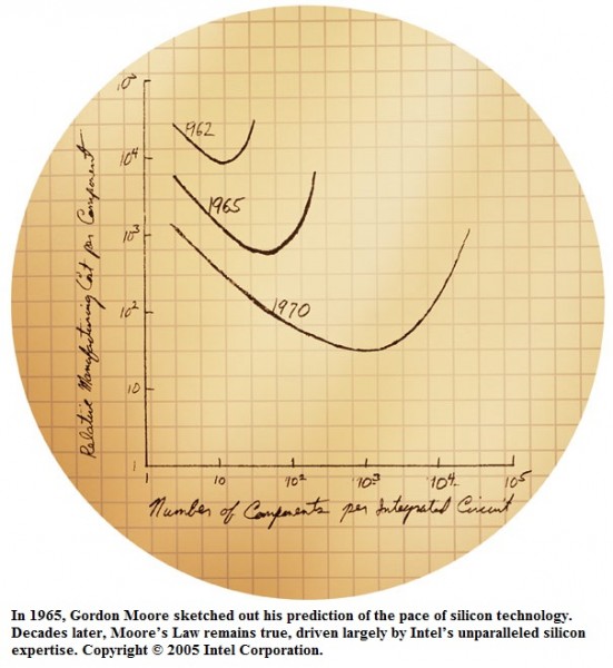
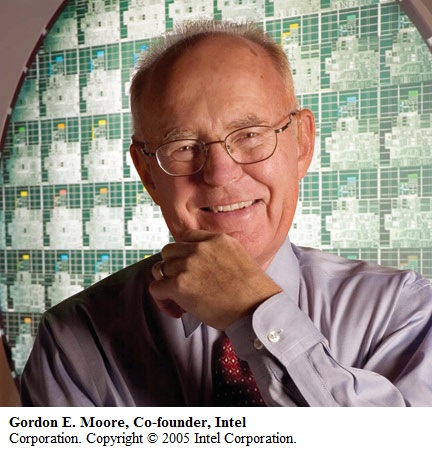
This trend was first observed by Intel co-founder Gordon Moore in 1965, and the term “Moore’s Law” was coined several years later. For over forty years this “law” has held, chips
have gotten more complex, and transistors have shrunk into the nanometer (nm) range.
Today, the traditional materials and production methods have been pushed to their limits. Concerns about leakage current and overheating have caused many insiders to question whether the industry could continue its trend of doubling the number of transistors on a chip every two years. They have warned that Moore’s Law may soon have to be repealed.
Leakage Current & Overheating
Integrated circuits use insulating materials to isolate the “gate” of the transistor from the silicon substrate. The gate is the electrode that, when energized, turns the transistor on and off. Current that “leaks” past the insulation is not just wasted energy, it results in unwanted heat.
Leakage current and the resulting heat generated have become more of a problem in recent years as transistor counts have continued to increase, and decreasing transistor sizes have approached the atomic level. The issue of “leakage current” increases exponentially as the number of transistors increases.
High-k/Metal Gate Materials
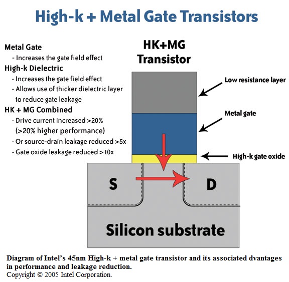
Intel Corporation has developed several new insulation materials for use in transistors which make up computer chips. These new materials replace the silicon dioxide dielectric material which has been used for over 40 years. Researchers use the term “high-k” to describe materials that have a dielectric constant – or ‘k’ value – higher than 3.9k, the dielectric constant of silicon dioxide. Air is the reference point for dielectric constants and has a value of 1. These new materials are known to include various alloys of Hafnium, but the actual metals used are a trade secret.
The high-k dielectric is one of many steps that have been pioneered to help alleviate heat problems and promise to reduce leakage current 100 fold. The use of high-k material has also required that a new, compatible material be found for the transistor’s electrode. This new electrode is referred to as a ‘metal gate’ and it replaces the polysilicon gate electrode material that has also been used for many years. The working combination of the high-k dielectric and the metal gate is perhaps the most important breakthrough in transistor design in forty years.
“Implementation of high-k and metal materials marks the biggest change in transistor technology since introduction of the polysilicon gate MOS transistors in the late 1960s,” says Gordon Moore.
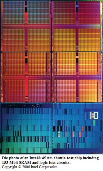
Intel is confident that the new technology will allow transistors to continue to shrink, and allow the industry to continue the 2-year-cycle of Moore’s law for several additional generations of microprocessors. The first application of the technology will be in a 45nm transistor. For reference, a nanometer is one billionth of a meter. See the sidebar for some interesting facts about just how small a 45nm transistor is. Just ten years ago a state of the art transistor was 250nm (5.5x the size and 30x the area of a 45nm device).
Further good news from Intel indicates that the new transistor technology can be produced using techniques similar to the techniques in use today at their existing “fabs” (semiconductor manufacturers refer to their factories as “fabs”) and without having to completely re-engineer the fabrication process. Production parts are expected to ship in 2007 and actual CPUs could be available in early 2008.
Intel announced in mid January that the first 45nm architecture – “Penryn” – has been successfully tested with several operating systems, including Windows Vista, Windows XP, MacOS X and Linux. Penryn will form the basis of several CPUs, with code names like Wolfdale, Yorkfield, and Montevinia. The dual core Penryn processors will contain 410 million transistors, while the quad-core versions will contain over 800 million.
3-D Chips
Another technical breakthrough has been announced by IBM. To date, all connections to computer chips are made around the perimeter of the chip. It’s common knowledge that many semiconductor companies have been working on methods of connecting chips in a vertical manner. IBM has been working on the concept for more than 10 years.

IBM’s new method allows holes to be etched all the way through the chip, called “through-silicon-vias,” which are then injected with tungsten to create wires and electrical connections within the chip. The breakthrough is believed to be “production ready”, meaning that it would be useful beyond the lab and achievable in a production environment within the next year.
“This breakthrough is a result of more than a decade of pioneering research at IBM,” said Lisa Su, vice president, Semiconductor Research and Development Center, IBM. “This allows us to move 3-D chips from the ‘lab to the fab’ across a range of applications.”
The vertical connections will allow micro-processors to be stacked on top of other chips, such as memory chips. Thus the connection distances between the chips can be reduced, resulting in faster communications between the chips. According to IBM, the technique shortens the distance information needs to travel by 1000 times, and will allow the addition of up to 100 times more channels, or pathways, for that information to flow compared to
2-D chips.
The new stacked chip configuration is also touted to reduce heat dissipation and power usage. IBM claims that the ‘through-silicon-via’ can improve power efficiency up to 40% – a huge benefit for battery-operated devices, such as cell phones and laptops. The breakthrough will also allow advances for the multi-core processors that have been proliferating lately. These dual-core and quad-core devices are limited by their current ‘vertical only’ implementations, and the 3-D technology can put power closer to each core, increasing the speed of the processor and reducing power consumption by 20%, according to IBM. It may also be pivotal in the development of larger scale, multi-core processors with 8, 16 or more cores.
By: Chip McDaniel (a bigger, slower Chip)
AutomationDirect
For more information:
Intel’s Technology and Research page:
http://www.intel.com/technology/
IBM’s press release on the 3-D technology
http://www-03.ibm.com/press/us/en/pressrelease/21350.wss
Moore’s Law
http://www.intel.com/technology/mooreslaw/index.htm
http://en.wikipedia.org/wiki/Moore’s_law
Originally Published: June 1, 2007


